2021
August 05: ESP and solar panel Part 2; the results2020
December 26: ESP and solar panel Part 1; the setup August 22: ESP-8266 power issue with ME6206 regulator2019
October 18: How to use alarm syscall in Ruby2018
December 20: Decode Oregon Scientific sensors with RaspberryPi and Arduino2016
October 19: How I recovered a dead hard drive with a freezer September 28: Drawing a ground plane in Kicad June 27: Quick Ruby On Rail memo2015
December 18: Signal handling and Ruby December 14: EventMachine is good but... September 18: My custom ortholinear keyboard February 08: Quick Sinatra boilerplate2014
September 16: Wifi access point on a Raspberry Pi March 24: Linphone and G729 on Opensuse2013
November 11: Ext4 rescue tips November 05: Why this blog is'nt running Wordpress ?Drawing a ground plane in Kicad
- September 28, 2016
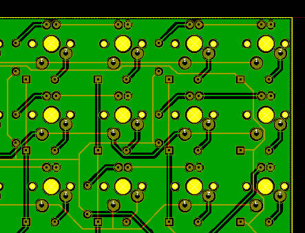
While designing the PCB of my next keyboard in Kicad, I was looking for a way to create a ground plane. Half of the tracks on this board will carry around 300mA with a PWM signal, so it could be a good idea.
Creating a ground plane manually in Kicad is simple, the Zone tool is quite straightforward. But with an external auto router like FreeRouting it's not so easy, moreover if there is a lots of tracks on both side of the PCB. The ground plane must be filled in after all tracks have been placed. If you do it before, FreeRouting will ignore it and generate useless data.
How to do it ?
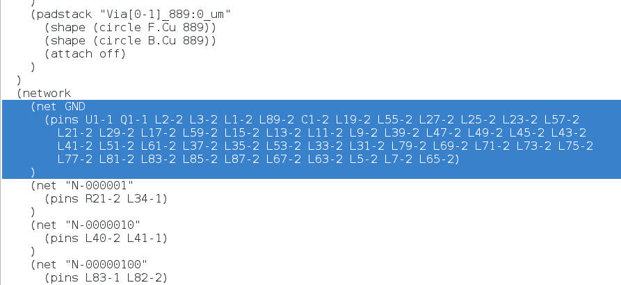
The first step is to remove the ground network from the Specctra DSN file, so FreeRouting does not touch it. Generate the .dsn file with the tool located in Tool -> Freeroute. Then edit this file with a text editor and remove the GND block in the Network section, like on this screenshot :
Once done, you can load the file in FreeRouting and launch the routing. It may be necessary to adjust few parameters of the router to give a higher cost to the tracks on the back side. This will help to avoid island, ie. part of the ground plane not connected to anything. These settings are in Parameter -> Autoroute -> Detail.
Then, you can load back the Specctra SES file into Kicad, draw the zone on the back side of the board and fill it. Use the DRC check to verify there is no unconnected pin, which would indicate an island on the groud plane. In that case it will require a manual fix and fill the zone again, but that's much less work than doing everything by hand !